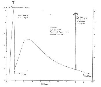
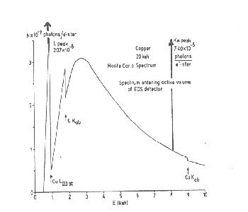
Typical EDS detector is illustrated in figure 1. When X-ray comes to detector they must pass through a Be windows (nominal thickness of 7.6 microns), a gold surface electrode (thickness of about 20 nm) and an inactive or dead layer of Si (thickness of 20 - 200 nm). The absorption which occurs during passage through those layers eliminates virtually all X-rays with energy below 500 eV. Above an energy of about 2 keV the absorption becomes relatively insignificant so that nearly all X-rays pass into active layer of detector (thickness obout 3 mm). Figure 2 and 3 shows EDS spectrum calculated by Monte Carlo method without and with absorption.
Figure 1: Structure of typical Si(Li) EDS detector.
Figure 2: Characteristic and continuum X-ray spectrum emitted from bulk Cu sample, excited with 20 keV electrons, calculated by Monte Carlo method and figure 4, experimental EDS spectrum.
Figure 3: Spectrum of Fig. 2 corrected for absorption in the Be window and Si dead layer.
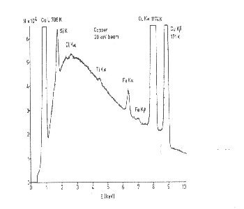
Figure 4: Experimental spectrum of Cu, 20 keV. Cl, Ti, and Fe are trace contaminants in the specimen or or mounting media. Note that the Cu K alpha escape peak at 6.40 keV.