The SEM instrument has many applications across different industry sectors. The extremely high magnification images together with localised chemical information means the instrument is capable of solving a great deal of common industrial issues such as particle analysis, defect identification materials and metallurgical problems.
Energy Dispersive X-ray Spectroscopy (EDS) is an analytical capability that can be coupled with several applications including Scanning Electron Microscopy (SEM), Transmission Electron Microscopy (TEM) and Scanning Transmission Electron Microscopy (STEM). EDS, when combined with these imaging tools, can provide elemental analysis on areas as small as nanometers in diameter. The impact of the electron beam on
the sample produces x-rays that are characteristic of the elements found on the sample. With EDS, you can determine the elemental composition of individual points or map out the lateral distribution of elements from select areas.
Technological progress has been strongly influenced by the creation of new materials and further developments of existing materials. As the macro properties of a material are dedicted by its micro properties (phase distribution, grain size and shape; as well as inhomogeneties such as inclusions, segregation and porosity) it is important to know and understand the microstructure of material. The scanning electron microscope (SEM) is particulary suited for this purpose.
Most inspections start with magnifications of the specimen surface using secondary electron signal. Composite materials or materials where inhomogenity is very important, can be investigated using backscatter signal. Microanalysis can then be applied to obtain identificatin and quantification of the element cmposition. In this way, particles down to small (submicron) sizes, thin layers as well as bulk material, can be fully analysed. Here is a few examples of our analysis capability.
Scanning Electron Microscopy
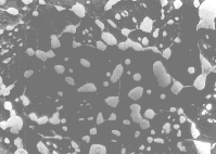
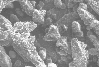
Scanning electron microscope is one of the basic tools for development of new and control of existing materials. With very wide magnification range (10 X to 200 000 X) is very suitable for imaging different phases in the mistrostructures.
The upper image show spheroidized perlite in hyper-eutected steel (1 wt.% C) with Fe
3C near spherical particles in the ferrite matrix.
EDS Microanalysis
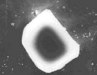
Inclusions control (composition, shape and distribution) is one of the most important task in the steelmaking production. Most common inclusions in the steels are sulphide and oxide inclusions of different shapes and sizes. The left image show Ti(C, N) inclusion in the matrix of the nickel base alloy Nimonic 80A. Size of this inclusion is 3 microns and EDS specter shows presence of C, N and Ti.
Image Analysis
In many applications that involved processing of materials, the average grain size, inclusion and particle size needs to be determined. One reason is to ensure the material's strength. Generally, the smaller are this features, the stronger the material. This features may be determined manually or with the use of an image analysis. There are many image analysis programs, but we used one of the best, NIH-Image.
Thin Film Analysis
The strength of nickel base alloys primary depends on size and distribution of gamma prime percipitates. The left image show gamma prime percipitates in the carbon extraction replica of the nickel alloy Nimonic 80A. Percipitates has a avarage diameter of 300 A. EDS microanalysis shows that the composition of this gamma prime percipitates is 11.99 wt.% Al, 13.36 wt.% Ti and 74.82 wt.% Ni and is very closly to the stehiometric composition of Ni
3AlTi phase in this alloy.
Failure Analysis
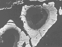
Scanning eletron microscope is versatile and useful tool for failure analysis (high resolution, wide magnification range and very large depth of field, simple specimen preparation and possibility of microanalysis). The left image show tipical casting defects - shrinkageholes in the cast part, which was broken during in service.
Nonmetallic Sample Analysis
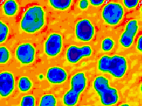
The intensity of backscattered electrons is largly dependant on the atomic number (Z) of elements. that constitute sample. Backscattered electrons can be largly used for compositional imaging (Z-contrast) of the multi-phase samples, such as ceramics, minerals, slags, etc., becasue they shows differences in the sample compostion. In this image of the mineral sample, can be distinguish four different compostions areas SiO
2 (Z=10.76), CaSiO
4 (Z=13.45), Ca
2Si
2O
7 (Z=14.02) and Ca
2SiO
4 (Z=14.40).
Environmental Samples Analysis
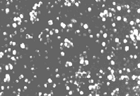
Scanning electron microscopy and microanalysis are successfully used nowdays in analysis different particles in the air and in the water. The images shows air particles collected with filter paper in the steel plant production site. Size of particles is from 1 to 0.1 microns with average composition in weight %: 3.933 wt.% Mg, 5.247 wt.% Si, 11.787 wt.% S, 15.642 wt.% Ca 2.862 wt.% Cr, 11.748 wt.% Mn and 48.780 wt.% Fe.
Consulting Service
- General microscopy & microanalysis consulting
- On-site microscopy & microanalysis training
- Equipment selection consulting
- Computer programming & data analysis
- Internet consulting
- Internet publishing & WWW services
- Steel technical data service
Production Problem Solving
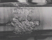
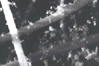
In cold steel rolling, the rolls have palyed the dominant role in rolling technology. During cold rolling are on cold rolls appeared defects like cracks, grinding network, spalling, hair cracks, crushing of roll surface, welding spots, roll failure, corrosion pits, retempered structure, etc. The image shows tipical defect of crushing of the roll surface on roll made from steel with 6 wt.% of Cr and diameter of 129 mm.
Monte Carlo Simulation
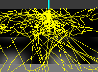
Monte Carlo modeling software produces visual models of electron beam/ specimen interactins for scanning or transmission electron microscopy. Any sample chemistry can be modeled. Model bulk materials, standalone thin films, or films on substrate and inclusions in the matrix. The image shows primary electron interaction volume in the hipotetic thin film sample with Au, Cu steel layers thickness of 1000 A at 20 kV and 0 degrees of tilt angle.