|
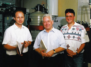
| Part of the R&D team of the Thin Films and Surfaces Department: Dr Peter Panjan (research fellow), Prof. Dr Boris Navinsek (head of the Department) and Josko Fiser (technician). |
by Boris Navinsek and Peter Panjan
Part of the R&D team of the Thin Films and Surfaces Department: Dr Peter Panjan (research fellow), Prof. Dr Boris Navinsek (head of the Department) and Josko Fiser (technician).
The activities of the Department
of Thin Films and Surfaces are basic and applied research of thin
film technologies, one of the most promising areas of materials
science. Many areas of modern technology are directly affected
by thin film science. For example, silicon integrated circuits
form the basis for the computing and telecommunications industries;
oxide thin film multilayer structures are used in optics and electrooptics;
ceramic thin films are very important as wear, corrosion and oxidation
resistant coatings, etc.
In 1960, we started to use sputtering techniques for preparing
a wide spectrum of metal thin films and their nitrides, oxides
and carbides in the form of single and multilayer structures.
This deposition technique, also called Physical Vapour Deposition
(PVD), or reactive plasma deposition, is still today the basic
technology for world wide applications of thin films in microelectronics,
electronic component manufacturing, in optics and optoelectronics,
information technologies and tribology. This last field of research
has been a major high-tech area from the industrial application
point of view in the last 15 years, and is generally known in
Europe as “Plasma and Ion Surface Engineering” (PISE).
Our research in electronics and microelectronics has included
deposition and characterization of various thin film resistors
(NiCr, Ta2N, NiCrAl), transparent conductive Indium Tin Oxide
(ITO) films, metallization structures for VLSI circuits (<Si>-TiSi2/TiN/Al),
transition metal silicides and aluminides (e.g. TiSi2, ZrSi2,
CoSi2, CrSi2, NiAl), ferroelectric LiTaO3 thin films, high temperature
superconducting films type YBaCuO and superconducting multilayer
systems type YBaCuO/NiO and YBaCuO/ZrO2. Recently, Yttrium Stabilized
Zirconia (YSZ) thin films, to be used in fuel cells, have also
been studied and developed.

|
Prof. Dr Boris Navinsek, Head of IJS Department of Thin Films and Surfaces |
15 years ago our Department
started systematically to study and develop various types of hard,
wear, corrosion and oxidation resistant coatings. The following
four research area are included within this program, which is
also a part of European joint PISE and COST 515 projects,:
• Ion and plasma interactions with solid surfaces, including
the study of interactions during ion etching and thermal annealing.
• Synthesis of new wear, oxidation and corrosion resistant
coatings (metallurgical coatings).
• Study of interface interaction in bi- and multilayer structures
during thermal annealing and preparation of Standard Reference
Materials (SRM) in the form of multilayer structures, to be used
for depth profile analysis in surface physics.
• Development and industrial application of new PVD “clean
technologies”, which will be used very soon to replace traditional
galvanic coatings.
• We have the most modern deposition equipments, measuring
techniques and analytical instruments for all these research programs.
There is also a Hard Coating Center within the Department, where
hard protective coatings are developed for industrial applications.
The selection of optimum tooling
is the most important activity in today’s successful development
of machine work in all industries, especially where metal cutting,
cold forming and forging processes are involved. A remarkable
tool life improvement, better surface quality of products and
higher productivity has been obtained by using hard and protective
PVD coatings.
Titanium nitride (TiN) coating, 2-5 mm thick, with a microhardness
of 2000 HV0.025, was the first generation of PVD coatings. It
was introduced in 1980, and has been used all around the world
ever since. At our Department we also developed our own TiN technology,
known as JOSTiN (the trademark is registered in 23 countries,
and it is produced in BAI 730 and BAI 730M Balzers equipment in
our Hard Coating Center in Domzale.
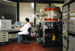
A view of the Hard Coating Center (Domzale); one of the low voltage plasma beam apparatus BAI 730M (Balzers) for production of hard protective coatings equipped with the Plasma Process Monitor PPM421 (Balzers) to be used for plasma diagnostics.
The second generation includes
titanium carbonitride (TiCN), chromium nitride (CrN) and titanium-aluminium
nitride (TiAlN). Because of their high hardness, of 3000 HV0.025,
TiCN and TiAlN are regarded as very high wear and abrasion resistant
coatings, while CrN and TiAlN are the only high temperature resistant
coatings that can be used up to a working temperature of 700-850°C.
The CrN coating has also been investigated extensively in the
last five years in our Department. Many results of the novel applications
in practice show that CrN is accepted today as a hard and protective
coating, which is successfully applied not only for selected tribo-systems,
but also as an excellent corrosion and high wear protection. We
have recently also developed a TiAlN coating, and the first tests
in hot forging of steel parts have already been completed. This
process, hot forging (parts with 1150°C), will be one of the
most complicated in practice for any improvement of moulds. Duplex
coatings - a combination of plasma nitriding and TiAlN coating
- could be a solution.
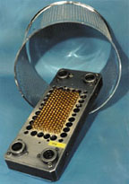
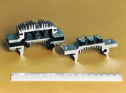
TiN coated high speed steel (HSS) cutting tools used for perforation of drums in a washing machine, Gorenje, Velenje.
Finally, the third generation of PVD coatings includes new fields of research and applications in PVD hard coatings, such as diamond and diamond like carbon (DLC) coatings, to be used for the machining of e.g. graphite, glassfaser, woods and soft materials, multilayered and multicomponent coatings (e.g. TiCrN, TiZrN, TiVN, CrAlN, TiAlVN etc.) and polycrystalline superlattice coatings (for special machining operations). TiN/CrN, TiN/Ti/TiN, ZrN/Zr/ZrN and TiN/ZrN multilayered coating have been studied and characterized in our Department. All these multilayered coatings show unexpectedly high microhardness and new physical, chemical, corrosion and oxidation properties. We should also mention the double coatings TiN+CrN, which have already shown very high wear and abrasive resistance in practice.
|
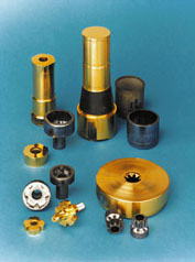
TiN coated cold forming tools and products, used in the manufacturing of components in Iskra Avtoelektrika, Nova Gorica |
Conventional PVD coatings are
deposited at temperatures between 400 and 480°C. These temperatures
are ideal for the majority of industrial applications, whereby
optimal microstructural and functional coating characteristics
can be obtained. For many standard tool materials, which are sensitive
to temperatures higher than 250°C (e.g. AISI D2 or D3), the
usual temperature of deposition is too high. For those materials,
a low temperature PVD process has been developed, using our plasma
beam sputtering machine SPUTRON DC/RF. The development of low
temperature coatings with good functional characteristic is not
easy, since a reduction of the coating temperature normally results
in unhomogeneous coatings and reduced coating adhesion. We discovered
that the CrN coating is characterized by its fine grained and
low internal stress structure, which permits deposition of the
most uncomplicated coating system of all four coatings (TiN, TiCN,
CrN, TiAlN). This technology allows us to deposit coatings with
much larger thicknesses than conventional PVD coatings of a few
µm. In various novel industrial applications, we have shown
that CrN has successful adhesion to steel substrate as well as
excellent corrosion and oxidation resistance. Adhesion to tool
steel substrate (and also to other inexpensive construction steels)
was improved by the deposition of a 0.1-0.5 µm thick Cr
intermediate layer, which helps to form an optimum width of the
interface, as was clearly observed by AES, XPS and GDOS depth
profile analysis. The technology of CrN coating preparation has
been patented by our department. The thickness of CrN coatings
for industrial application depend on the tribo-system and could
be between 3-10 µm.
CrN coating have been used in Slovenia for selected applications
such as wear and corrosion protection of tools in cold forming
and cutting copper in commutator manufacturing, in forming aluminum
and steel components in automotive production and for surface
improvement of moulds in Al-Si die casting under pressure.
The lowest obtainable temperature of 140°C in the SPUTRON
apparatus gave a CrN coating of high quality for practical use.
These coatings were used to protect electrodeposited and electropolished
Ni moulds for artificial teeth production.
Double TiN+CrN coatings are also regularly used as a highly abrasive
and wear resistant coating in the production of rotors in the
Slovenian electromotor industry.
The low temperature hard coatings are also used for protection
of easily machined and cheap low temperature substrates, as substitute
products for more expensive components and for decorative purposes
on substrates such as chrome-plated brass and die-cast zinc parts.

Cutting and forming tools coated with TiN hard protective coating (JOSTiN®)
Study of metallurgical coatings
is a typical multidisciplinary field of research involving the
physics of thin films and surfaces, plasma physics, material science,
chemistry and corrosion, metallurgy, machine engineering and tribology.
From a tribological point of view, the most important properties
of hard coating are microhardness, adhesion, oxidation and corrosion
resistance, thermal conductivity and the friction coefficient
of the tool material vs. workpiece material. All these properties
are closely related to the basic material properties. So a complete
characterization of hard coatings is necessary. Such study includes
complex characterization methods which are available in our Department
and also in the Ceramics Department and Department of physical
and organic chemistry at the Jozef Stefan Institute:
• Determination of basic physical properties of films and
coatings: microstructure, lattice parameters, surface morphology,
microhardness, adhesion, friction and scratching coefficient,
electrical and optical properties.
• Study of corrosion and passivisation behaviour of coatings
by electrochemical and surface analytical techniques XPS, SEM
and AES.
• Investigation of oxidation mechanisms of hard coatings
by measuring oxidation resistance and activation energy of oxidation.
• Performance tests in industrial conditions show improvement
of tool life at room and at elevated temperatures (up to 800°C),
surface quality of products, and optimization of tribo-systems
in various industrial manufacturing.

Cross-sectional transmission electron micrograph of multilayered Ni/Cr/Cr2O3 Standard Reference Material (SRM) deposited onto polished silicon wafer, developed at the request of Bodenseewerk Perkin GmbH (Munich)
Basic research has been concentrated
for more than 20 years on the development and characterization
of sputtered thin films and their interaction with various substrate
materials. In addition to the general properties of thin films,
we have also studied interface interactions during annealing of
various bilayers and multilayers, using different experimental
techniques (AES, TEM, TDS).
Owing to the disequilibrium condition of the technological procedure
of preparation, thin films and multilayer structures contain a
high concentration of structural defects. In practice, they are
also operated at high current density (e.g. very large scale integrated
circuits), radiation load (e.g. laser and sinchrotron mirrors),
and very high temperature and mechanical load (e.g. hard coatings).
So such systems try to obtain the equilibrium stage by transport
of materials and chemical reactions between discrete layers or
phases. From the application point of view, it is very important
to predict the thermal stability of such a structure.
The solid-phase reactions of thin films in multilayer structures
during thermal annealing are generally detrimental, but on the
other hand, such reaction can very often be beneficial, while
this is the easiest method of preparation of some compounds, such
as transition metal silicides and various intermetallic phases.
Owing to the many interfaces, the interfacial reaction in multilayer
structures is faster than in bilayer and the new phase can be
prepared at a lower annealing temperature. By controlling the
experimental parameters, material scientists can prepare specific
phases with desirable properties. In cooperation with the research
groups of the Institute for Surface Engineering and Optoelectronics
(Ljubljana) and the Max-Planck Institut für Metallforschung
(Stuttgart, Germany) we have been investigating the interfacial
reactions in various Me/Si and Me/Me bi- and multilayer structures:
Ni/Si, Al/Si, Cr/Si, Co/Si, W/Si, Mo/Si, Nb/Si, Ni/Cr, Ni/Cr/
/Cr2O3, NiO/Cr2O3, Fe/Al, Ni/Al. Using different experimental
techniques we investigated: (a) the phase formation sequence,
(b) the kinetics of phase formation and (c) the main migrating
elements of the reactions.

Adhesion tester (Automatic scratcher tester, CSMS Revetest, Neuchatel, Schwitzerland)
For the last 15 years, we have
also been investigating various multilayered structures (MLS)
appropriate as standard reference materials (SRM) for surface
analytical techniques. We need such standards for calibration
a sputter time scale of depth profile techniques, as well as for
the optimization of conditions of analysis. MLS appropriate for
such standard must as far as possible fulfil the following structural
requirements: a) films must have an amorphous or very fine microstructure,
b) film density must be close to bulk density, c) impurities content
at interfaces and in the films must be as low as possible and
e) the interface must be as smooth as possible.
At the request of NIST (NBS), Washington, in 1984-1986 we developed,
manufactured and characterized the standard reference materials
SRM 2135 and SRM 2136 for surface analysis in the form of a Ni-Cr
and Cr/Cr2O3 multilayer on Si(100) wafers. A similar SRM in the
form of a Cr/Ni/Cr2O3/Cr/Ni multilayer structure was also made
at the request of Bodenseewerk Perkin-Elmer GmbH (Munich). In
cooperation with the research groups of the Institute for Surface
Engineering and Optoelectronics (Ljubljana) and the Max-Planck
Institut für Metallforschung (Stuttgart, Germany) we also
investigated the influence of diffusion, segregation, reaction
at the interface and sputter parameters on depth resolution of
AES, XPS and secondary ion mass (SIMS) depth profile techniques.
Three years ago, an interlaboratory comparison (round robin experiment)
of depth profiling results for Ni/Cr multilayer using AES, XPS
and SIMS was organized between four laboratories.
The two standards are the only available multilayers in the world
which are still in use for the calibration of depth profile analysis
in AES, SIMS and XPS surface characterization. We also develop
and characterize new SRM for hard coatings, using an AES depth
profile technique, Rutherford backscattering spectrometry (RBS)
and cross sectional transmission electron microscopy.
We recently introduced the first research in Slovenia on an extremely important industrial application of thin films and coatings, also known as “replacement of galvanic coatings with plasma (PVD) metallic and ceramics coatings”. Electroplated and electroless coatings are commonly used to protect surfaces from corrosion and wear, as well as for decorative purposes. However, both traditional techniques are also a major source of environmental pollution. So the development of alternative clean technologies in all spheres of industrial manufacturing is a worthwhile task today in industrially well developed countries in the world. Owing to major ecological problems, the situation has changed dramatically in recent years. There is no doubt that in the next 3 to 5, or at the least 10 years, many galvanic coating processes will not be allowed in most industrial manufacturing. In the last five years, PVD metallic and ceramic hard protective coatings have already been used for the replacement of galvanic coatings in some specific applications. Replacing such traditional technology requires far more than simply demonstrating that modern alternatives can perform as well or even better. Today, it looks at first sight impossible to compare prices of galvanic coatings against PVD coatings. The only reason now is low production volume. But if production costs are calculated on the basis of the same production volume, and all relevant costs are properly taken into account for the entire production process (including finishing), modern PVD methods are frequently competitive with older electroplating methods, or even less expensive, especially if one takes into account large mass production and improved performance of alternative coatings. However, ecology is already today dictating the prices of many manufacturing processes. In some countries, regional environmental ordinances have become so strict that industry will be forced to replace electroless and electrodeposited coatings, such as Ni, Zn, Cd, Cr, Au and many metals and alloys. However, there are still many problems with PVD technologies that coater designers and manufacturers must solve in the near future. Some of them are:
• the quantity of parts
and components to be coated is large: from a few 100,000 to a
few millions, made of the same material and having the same size,
• the size (and not simple geometry) of the parts and components
varies from a few mm to a few hundred cm,
• PVD coatings require a cleaner surface than galvanic processes
(plasma cleaning is needed),
• the PVD coatings to be used for replacement of galvanic
coatings are quite complicated and not easily incorporated into
many production environments. They are available in a new coating
centers and the price will depend on the future arrangement of
specially designed flexible, high-output or on-line systems.
The Department of Thin Films and Surfaces, together with Iskra
Avtoelektrika, the largest Slovenian manufacturer of starters
and alternators, as a partner from industry, and Ballzers A.G.,
Liechtenstein, has already completed the first phase of a new
clean technology replacing nickel and hard chrome with PVD coating,
sputtered nickel and CrN coating, respectively. Both tests in
production conditions were positive. We now plan to build a Center
of alternative PVD technologies, using high output sputtering
equipment.
Recently, the first phase of the project “Replacement of galvanic nickel and hard chrome with PVD coatings” was completed in cooperation with Iskra Avtoelektrika and Balzers, Liechtenstein. The photograph shows the cooling bodies of diodes, part of an automotive alternator coated with PVD nickel to assure good soldering.
Applied research is a very
important activity of the IJS Department of Thin Films and Surfaces.
Our department includes also the Hard Coatings Center (Domzale),
established in 1985 in cooperation with SMELT, Ljubljana and Balzers
AG Wear Protection, from Liechtenstein, to develop new metallurgical
coatings for industrial applications and to serve industrial needs.
In the last ten years, more than 4,000,000 pieces of tools and
machine parts for machine, electrical, wood and other industries
have been protected with TiN and CrN hard, corrosion and oxidation
resistant coatings.
Tools and machine parts have been coated for more than 300 manufacturers
in Slovenia, as well as abroad. Systematic analysis of performance
tests in industry has been performed using tools protected with
our TiN (JOSTiN®) technology and CrN coatings in the Slovenian
machine, electrical and wood industry. Production experts have
improved the productivity of these coatings and the quality of
the final products. These new technologies have also brought to
Slovenia better business and the advantages that are required
from international institutions giving ISO 9001 certificates to
our industrial manufacturers.

|
| The organization of educational courses for technical personnel from industry is also a very important activity of our Department. More than 150 participants from industry and institutes attend specialized seminars, organized every 4 years. |